|
|
|
The manufactoring and characterization of smallest structures play a key role in the field of modern micro-/nanoelectronics and related areas. Systems for ion beam milling utilizing a focuses ion beam (FIB) become increasingly important. These systems have been commercially available for more than ten years mostly applied in semiconductor research. More recently, FIB technology has supported development of next-generation microelectronic devices1, microelectromechanical systems (MEMS)2,3, research into novel materials4,5, and manufacturing of scanning probe tips6,7. Application examples include transmission electron microscope (TEM) sample preparation8, failure analysis of semiconductor devices9,10, integrated circuit device repair11, maskless focused ion beam lithography12, and ion beam assisted deposition13. An excellent overview on the fundamental principles and applications is given by Melngailis14 and more recently by Reyntjens and Puers15. The fundamental operation principle of FIB systems is comparable to scanning electron microscopes (SEM). However, instead of an electron beam, a finely focused beam of ions with a diameter down to approx. 5 nm is applied. As shown schematically, an ion beam emitted from a liquid metal (alloy) field ionization source is focused onto the sample surface by a set of electrostatic lenses. In the case of an alloy ion source, a mass separator enables selection of the desired ionic species. Operating the primary ion beam at low beam currents allows imaging of the sample; at high beam currents sputtering or milling processes are induced.
Surface collision with energetic ions leads to sputtered material which leaves the surface either as secondary ions or neutral atoms (substrate milling). Furthermore, secondary electrons are generated at the surface. If the beam is scanned across the sample surface the signal generated by the secondary ions or electrons may be collected for imaging purposes with resolution in the nanometer range. At high primary ion beam currents significant material ablation is induced enabling precise milling, cutting drilling and structuring at the nanolevel. While e-beam lithography allows nanofabrication with higher lateral resolution, for many of the proposed applications short processing time (e.g. prototyping and characterization of novel devices and structures) and high throughput (e.g. TEM sample preparation) is an essential need. Among the most compelling features of the dualbeam instrumentation is the integration of field emission scanning electron microscopy and focused ion beam technology into one FIB/SEM system.
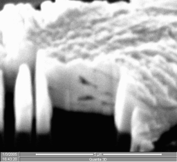
Two examples for FIB manufacturing left: Logo of the FIB2Center milled in a gold layer on silicon right: FIB-milling of a gold layer on silicon simultaneously observed with SEM
[1] F. A. Stevie, et. al., Surf. Interface Anal. 23, 61 (1995). |

|
[Martin Brucherseifer] [About me] [Resume] [SEM / FIB] [Scanning Probe Microscopy] [THz Spectroscopy] [AIXScan] [Publications] [Links] [Disclaimer] |